According to industry experts, the Indian VLSI industry requires anywhere be-tween 10,000 and 20,000 highly trained engineers at present. According to a joint report of India Semiconductor Association (ISA) and Ernst & Young, the semiconductor design industry in India is expected to log a compound annual growth rate of 17.3 per cent over the next three years to reach $10.6 billion.
There are a variety of career opportunities in product companies, design services companies and electronic design automation (EDA) companies. Product and application domains of VLSI include mobile and consumer electronics, computing, telecommunications and networking, data processing, automotive, healthcare and industrial applications.
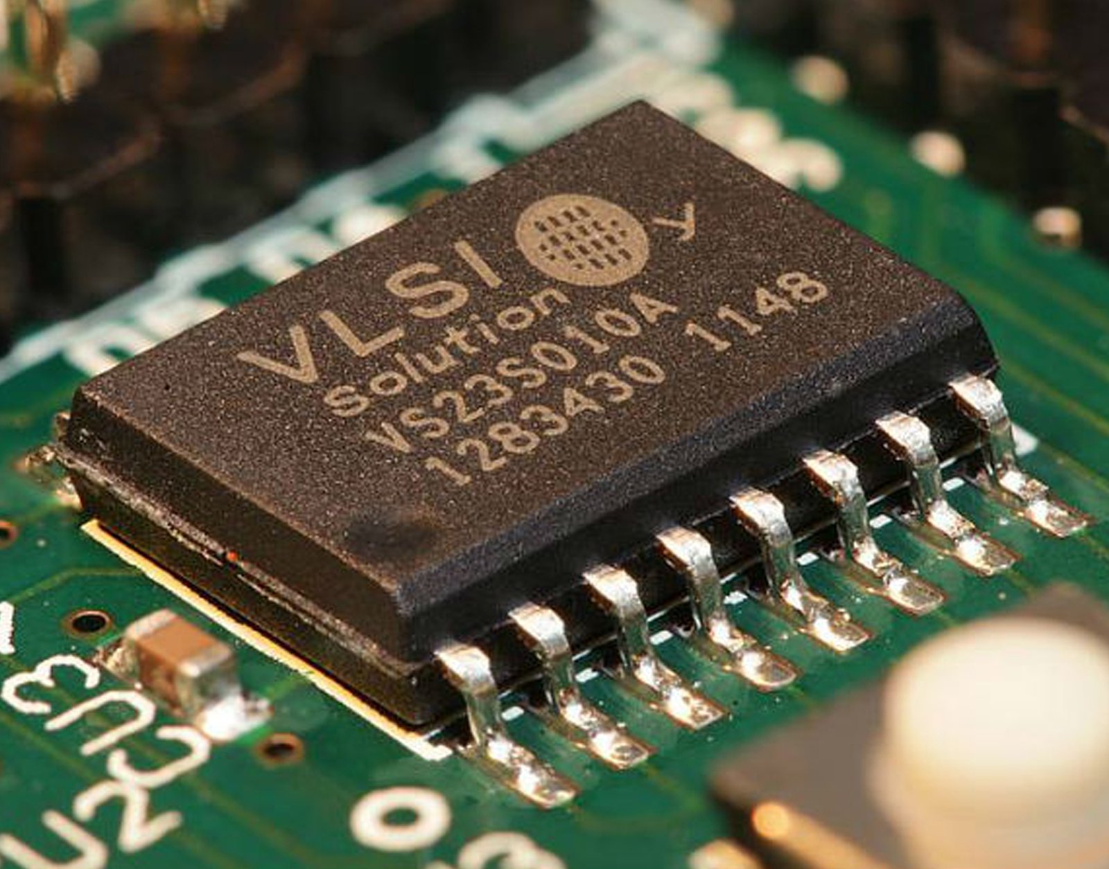
“In simple words, VLSI circuits are everywhere from your computer to your car, your brand new state-of-the-art digital camera, cellphones, and whatever electronics item you have,” says Kathuria.
Consumer demand for electronic products constitutes about 60 per cent of semiconductor sales today. With consumerisation comes the pressure to lower costs, retain product differ-entiation, manage volatile cycles and win the time-to-market race. “These pressures drive the demand for developing complex system-on-chip (SoC) devices, thereby creating a demand for VLSI skillsets,” affirms Vasudevan Aaghoramoorthy, vice president, semiconductor and systems, Wipro Technologies.
“Today, there is a huge demand in the industry for VLSI designers to develop field-programmable gate array (FPGA) implementations, application-specific integrated circuit (ASIC) designs and SoCs. The VLSI industry has an added attraction of being a strong domain for patents filing, invention disclosures and applied research,” he adds.
“There are a number of areas to choose in VLSI sector. One such area is reconfigurable computing. It is an interesting and pretty recent development in microelectronics that involves fabricating circuits which can be reprogrammed on the fly! And no, we are not talking about microcontrollers running with EEPROM inside. Reconfigurable computing involves specially fabricated FPGAs that when programmed act just like normal electronic circuits. These are designed such that by changing or reprogramming the connections between numerous sub-modules, the FPGAs can be made to behave like any circuit you wish.”